EVGA GeForce GTX 660 Ti FTW Signature 2 Review + SLI
Published by Christian Ney on 13.05.13Page:
Technical Data / Specifications
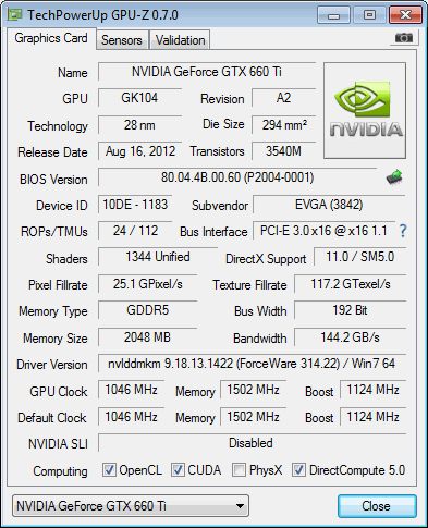
With the EVGA GeForce GTX 660 Ti FTW Signature 2 you get a factory overclocked card with a custom PCB cooled by a Signature 2 dual fan cooler. The ASIC quality measured on our sample was 86.2 % which is very high considering an average of 73 % on the cards we had in our hands.
About ASIC quality:

Looking at the clock speeds we see that the GPU runs at 1'046 MHz with a typical boost of 1'124 MHz, 144 MHz higher than the reference model. There are only two cards that feature higher clocks you can find in Europe. If you'd like to find them, check out our market overview: the DirectCU II Top from ASUS and the AMP! Extreme from Zotac. Like most other manufacturers no factory overclocking has been made on the GDDR5 memory, therefore the clocks remain at 1'500 MHz (6'000 MHz effective) following nVidia's recommendations.

| nVidia GeForce |
ASUS GTX 660 Ti DCU II Top |
EVGA GTX 660 Ti FTW S2 |
nVidia GF GTX 660 Ti |
| Chip | GK104 | GK104 | GK104 |
| Process | 28 nm | 28 nm | 28 nm |
| Transistors | 3.54 Billion | 3.54 billion | 3.54 billion |
| GPU clock | 1'059 MHz | 1'046 MHz | 915 MHz |
| GPU Boost clock | 1'137 MHz | 1'124 MHz | 980 MHz |
| Memory | 2'048 MB GDDR5 | 2'048 MB GDDR5 | 2'048 MB GDDR5 |
| Memory clock | 1'500 MHz (6'000 MHz) | 1'500 MHz (6'000 MHz) | 1'500 MHz (6'000 MHz) |
| Memory interface | 192 Bit | 192 Bit | 192 Bit |
| Memory bandwidth | 144'200 MB/s | 144'200 MB/s | 144'200 MB/s |
| TMUs | 112 | 112 | 112 |
| Shader Cores | 1'344 (7 SMX) | 1'344 (7 SMX) | 1'344 (7 SMX) |
| ROPs | 24 ROP | 24 ROP | 24 ROP |
| Maximum board power | XXX Watt | 150 Watt | 150 Watt |
| PCB Type | Custom Design | Custom Design | Reference Design |
| Size (PCB - Total) | 23.1 - 27.0 cm | 25.5 - 26.2 cm | XX.x - XX.x cm |
| Cooler | DirectCU II | Signature 2 | Reference Design |
| MSRP | $XXX | $319 | $299 |
As mentioned previously, this card from EVGA makes use of a custom PCB. But this PCB isn't unfamiliar, if you take a closer look you see that it's the GTX 680's reference PCB. Of course some minor changes have been made by EVGA's engineer team but you clearly see the ressemblance when comparing the PCBs one next to each other like on the picture below. Therefore you get an analog power design with six phases, where the GPU gets four phases and the memory gets two phase.
The voltage regulation chip used for the GPU here is a NCP5392P from ON Semiconductor. A bit different from the RT8802A (Richtek Technology) you find on the GTX 680 reference. On the memory power design side you find a chip labeled D7=ED SOZ.
This FTW card is available with two different coolers. There is also one with a blower type cooler close to the reference one. The one we are reviewing here is the dual fan version. The cooler consists of a nickel-plated two-section heatsink with a plastic shield and two 80 millimeter fans. The base as well as the four 8mm heatpipes are made from nickel-plated copper. The rest of the heatsink is made of nickel plated aluminium for a very neat look.
For those who care the two fans carry the part number PLA08015S12HH.
The memory chips used are made by Hynix and carry the model number H5GQ2H24AFR-R0C. They are specified to run at 1'500 MHz (6'000 MHz effective).
Discuss this article in the forums
| Navigate through the articles | |
 ASUS GeForce GTX 650 Ti Boost DirectCU II OC Review + SLI
 |
ASUS GTX 670 DirectCU Mini OC Review
 |
|
|


