Review: ASUS GeForce GTX 660 DirectCU II Top
Published by Christian Ney on 13.09.12Technical data / specifications
With the ASUS GeForce GTX 660 DirectCu II Top you get a factory overclocked card with a custom PCB design as well as a DirectCU II v2 cooler. The manufacturer claims that this baby is 8 % faster than the reference design, 78 % cooler and 3 times quieter. Thanks to the factory overclocking, binned GPU, custom cooler and reworked PCB design we can kind of believe that (not the 78 % cooler part though).
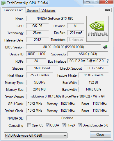
Looking at clock speeds we see that the GPU runs at 1'072 MHz standard with a
typical boost clock of 1'137 MHz. While the stock designed GTX 660 runs at
980 MHz with a boost of 1'033 MHz. Plus our sample was clocking itself up to
1'163
MHz which is 2x 13 MHz more than the specs. This time factory overclocking has
been made also regarding
the GDDR5 with a clock speed of 1'527 MHz (6'108 MHz effective) against nVidia's
recommendation of 1'500 MHz (6'000 MHz effective).
Now looking at the phycsical specifications of the DirectCU II Top version as
said before ASUS reworked the PCB, binned the core and used their own GPU cooler.
The DCU II Top gets 6 digital power phases and 3 POSCAP while the reference GTX
660 has only 4 analog phases and 1 POSCAP. You also find a lot of ASUS
technology that helps to improve overclocking, power efficiency, noise reduction
(less EMI), lifespan and so on. The DCU II Top version is powered by the DirectCU II cooler v2 (the v1
was crap if you ask me) which I literally love that features two 80mm fans with
11 blades each, three 6mm heatpipes and a red/black design. I was too lazy to
count the fins and calculate the dissipation surface/power but trust me, it's
big. So in other words to stay simple this graphics card is: Better, faster
and stronger.
| GeForce GTX 670 | GeForce GTX 660 Ti | ASUS GTX 660 DCU II Top | GeForce GTX 660 | |
| Chip | GK104 | GK104 | GK106 | GK106 |
| Process | 28 nm | 28 nm | 28 nm | 28 nm |
| Transistors | 3.54 billion | 3.54 billion | 2.54 billion | 2.54 billion |
| GPU clock | 915 MHz (Boost 980 MHz) | 915 MHz (Boost 980 MHz) | 1'072 MHz (Boost 1'137 MHz) | 980 MHz (Boost 1'033 MHz) |
| Memory | 2'048 MB GDDR5 | 2'048 MB GDDR5 | 2'048 MB GDDR5 | 2'048 MB GDDR5 |
| Memory clock | 6'000 MHz | 6'000 MHz | 6'108 MHz | 6'000 MHz |
| Memory interface | 256 Bit | 192 Bit | 192 Bit | 192 Bit |
| Memory bandwidth | 192'400 MB/s | 144'000 MB/s | 146'600 MB/s | 144'000 MB/s |
| TMUs | 112 | 112 | 80 | 80 |
| TAUs | -- | -- | -- | -- |
| Shader Cores | 1'344 (5D) | 1'344 (5D) | 960 (5D) | 960 (5D) |
| ROPs | 32 ROP | 24 ROP | 24 ROP | 24 ROP |
| Shader model | SM 5 | SM 5 | SM 5 | SM 5 |
| Maximum board power | 170 Watt | 150 Watt | 140 Watt | 140 Watt |
Discuss this article in the forums


| Navigate through the articles | |
 Review: ASUS GeForce GTX 660 Ti DirectCU II Top
 |
Review: EVGA GeForce GTX 650 Ti 2GB SSC SuperSuperClocked
 |
|
|